Chapter – 4
SIMULATION DETAILS OF THE PROJECT
In the past 10 years, photonic crystals (PCs) have attracted much scientific and commercial interest. The research and design work for PCs starts from accurate modal analysis of the device. Once the modes are found, structure can be simulated for that particular mode and the results of power spectra can be observed at the detector. In this chapter we will discuss about the modelling tool used for solving various problems related to photonic crystal device mentioned in next chapters. In our work, Opti-FDTD v11.0, a proprietary of Optiwave is used as a simulating tool to fulfill this purpose.
4.1 Introduction to FDTD
Opti-FDTD is a user-friendly graphical interface that allows the designing of photonic devices in an efficient manner. It provides accurate computer aided simulations with the proper analysis of results. It is a powerful and highly integrated software package which is based on the finite-difference time-domain (FDTD) method. FDTD technique implies the solution of maxwell equations with finite-difference expressions for the space and time derivatives. FDTD schemes are especially promising for the investigation of PBG structures, as they provide an opportunity of analyzing the spatial distribution of the electromagnetic field in PBG structure. Opti-FDTD enables to design, analyze and test nonlinear photonic components for wave propagation, scattering, reflection, diffraction and other nonlinear phenomenon. The method allows for the effective simulation and analysis of structures with sub-micron details. Such fine scale implies high degree of light confinement and a large refractive index contrast of materials to be used in design. Since FDTD method calculates electric and magnetic field at all points of computational domain, it is required for the domain to be finite. For this purpose, artificial boundaries are inserted in the simulation space. In FDTD perfectly matched layer (PML) acts as a absorbing layer for wave equations. In numerical methods, it truncates the computational regions while simulating problems.
4.2 Design Tools of Opti-FDTD
 Opti-FDTD is used to design photonic devices, simulate and analyze results. Design tools are available in toolbars and menu options. These tools include waveguide primitives, editing and manipulation tools, and special layout regions.
Fig 4.1. Main layout of Opti-FDTD Designer
Design tools of Opti-FDTD include designer, simulator and analyzer.
4.2.1 Opti-FDTD Designer
This section created the desired layout on a wafer that is saved in a file with the extension .fdt. Opti-FDTD designer is opened from the start menu. This section enables a user to work on multiple layouts of project at the same time. One can store and retrieve projects using .fdt files. In addition to the standard cut, copy, and paste editing functions, we can:
- Scale elements or groups of elements
- swap overlapping elements
- snap elements to a grid of the layout
- zoom into or out of the project layout
- link elements together
The main elements required to perform simulation of layout design include wafer, waveguide and input field.
 Wafer is the work area of design in Opti-FDTD. Each layout consists of only one wafer. It is a planar substrate on which we place and design the waveguides and cavities. The option of wafer properties is found in edit menu to modify the length, width and material of the wafer. Light wave propagates in Z-direction i.e. along the horizontal path on the screen. Discretization mesh is formed along the X-direction which corresponds to vertical path on the screen. Wafer is a necessary element for running a simulation. While starting a new project, the default material of wafer is air.
Fig 4.2. Wafer coordinate system
Waveguides are the building blocks of photonic circuits. Path perpendicular to the waveguide center defines the width of the waveguide. The default waveguide profile is air which can be changed while creating a new design. One can resize, rotate and move waveguides anywhere in the layout. Waveguide changes its color after selection. The orientation and shape of a waveguide can also be changed by dragging start/end handles. Properties of a waveguide can be viewed by double clicking it in the project layout. This opens the dialog box of waveguide properties where user can make required changes. Some major waveguide options provided by software include circular, elliptical and linear waveguides. From user point of view, waveguides can also be created by making some cells off in the photonic structure. Such a waveguide allows propagation of electromagnetic wave with minimum attenuation.
Get Help With Your Essay
If you need assistance with writing your essay, our professional essay writing service is here to help!
The input field is an essential element in design to allow simulation to run. Its position is at an input plane which can be moved throughout the layout. It defines the light that enters the simulated structure. Geometric position of the input field and its orientation can be defined in the input field dialog box. Options available for input fields in the software are modal, gaussian, rectangular and user defined. The concept of input field is purely geometrical. It is a position and direction which defines a plane completely. Multiple input fields can be positioned on multiple input fields simultaneously. In a 2D design, input plane can be horizontal (perpendicular to X-axis) or can be vertical (perpendicular to Z-axis).
Input field parameters must be defined carefully. The time domain parameters of input field
 can be specified as continuous wave or gaussian modulated continuous wave. Both the cases demand an input wavelength for the carrier wave. In Opti-FDTD all dimensions are defined in units of μm. Multiple input planes are distinguished with the help of ‘label’ facility provided by the software. Input wave can move in positive or negative direction depending on the option selected in the tab of wave configuration. An enable input field check box selects the input plane to be considered in calculation. Figures below show the placement of vertical and horizontal input plane.
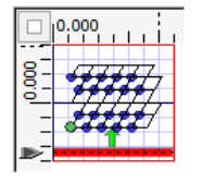 Fig 4.3. A vertical input plane for 2-D photonic crystal structure
Fig 4.4. A horizontal input plane for 2-D photonic crystal structure
Layout design in Opti-FDTD software includes profile designer, initial properties and layout designer. Profile designer define the material properties (refractive index of material) and channel profile. Initial properties set initial simulation domain properties including dimensions and material. Layout designer help to draw the lattice type (rectangular or hexagonal) and define the properties of the structure.
4.2.2 Opti-FDTD Simulator
Opti-FDTD provides two types of FDTD simulations
- 32-bit simulation (performed by 32-bit simulators)
- 64-bit simulation (performed by 64-bit simulators)
Opti-FDTD simulator monitors the progress, while the simulation is running. The simulation
 results are stored in a file with extension (.fda). After launching a 2-D simulation from Opti-FDTD designer, Opti-FDTD simulator displays the results of 2-D simulation. Fig. 4.5 shows the results of 2-D simulation for the structure shown in Fig. 4.3.
Fig 4.5. 2-D simulation results (image map) in Opti-FDTD simulator
Opti-FDTD simulator window contains output window and graph window.
4.2.2.1 Graph Window
 While running a 2-D simulation, a simulation window with several tabs appears. The first tab is the refractive index tab (Refr_Idx). Fig. 4.6 shows the refractive index distribution for the structure in Fig. 4.3.
Fig 4.6. Refractive index distribution (image map) with palette
Opti-FDTD simulator provides several types of views for graphs that include height plot and
 image map. Fig. 4.5 shows the image map of simulated field Ey. The height plot of the refractive index distribution of structure is shown in Fig. 4.7.
Fig 4.7. Height plot of refractive index distribution
4.2.2.2 Output Window
 The output window contains notification and error tabs which display notifications regarding the status of simulations or any error that occur during simulation. Opti-FDTD simulator does not show this window by default. It can be accessed from tools menu. Figure below shows an example of output window.


Fig 4.8. Output Window
Simulation parameters can be accessed in Opti-FDTD_Simulator by selecting simulation > simulation parameters. For changing any of the parameters one should use Opti-FDTD_Designer. These parameters can’t be changed in simulator.
Observation points can be used to obtain DFT and FFT transform. Observation line is used to observe power spectrum of the transmitted electromagnetic field.
 Opti-FDTD simulator provides the facility of PWE (plane wave expansion) solver.
Fig 4.9. Simulation parameters dialog box
Fig. 4.9. Simulation parameters dialog box
 The simulator provides tools for post-processing data analysis. Structure below shows the workflow of PBG structure analysis.
 Waveguide layout designer which provides necessary tools
for designing a PBG crystal structure.


 After designing, PWE band solver simulation parameters
are configured and PWE calculation is launched.


 After calculations results are automatically saved in .PND
file and data is used for post-processing analysis.
Fig. 4.10. Flow chart of PBG structure analysis
The PWE band solver contains two windows including band diagram graph window and processing image window. PWE band solver graph window displays data of each eigen values based on each k-vector. During simulation, data is updated continuously from currently running calculations. Progress of calculations can be seen in the window. After completion of calculations, band diagram can be plotted either as band-gap data graph or line-connected data point graph. Fig. 4.11 shows a PWE band solver graph display for the structure shown in Fig. 4.3.
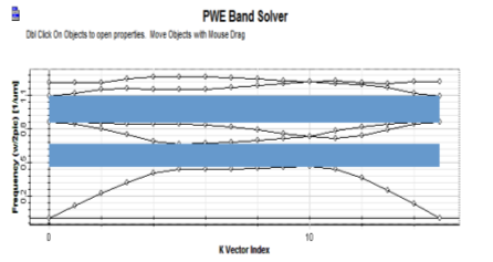
Fig. 4.11. PWE band solver graph window
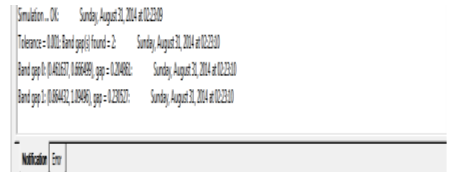 Processing message window consist of notification and error tabs. This window displays textual information related to the activities performed in band solver. It provides notification on the k-vector value, tolerance, iteration number and time and date when results were being observed. Fig. 4.12 shows the notification window for the above-mentioned band solver. Error window displays notifications about processing errors.


Fig. 4.12. Processing message window
4.2.3 Opti-FDTD Analyzer
Opti-FDTD provides the facility to view power spectrum. Observation points are used for this purpose. To view the spectrum, observation area analysis can be accessed from tools menu. Fig. 4.13 shows the observation area analysis dialog box.
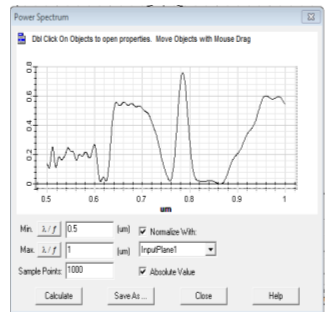
Fig. 4.13. Observation area analysis dialog box
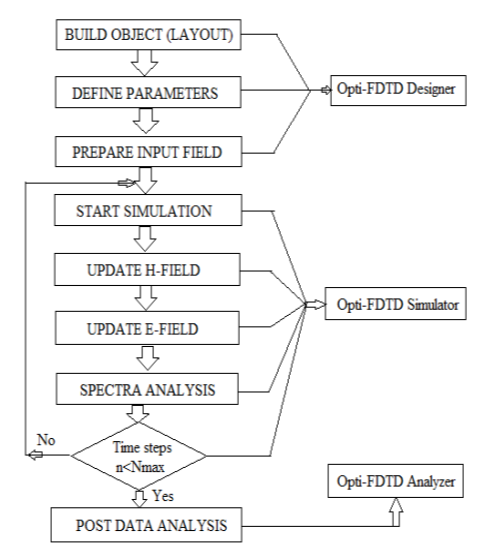
The flow chart below summarizes the full procedure of designing, simulating and analyzing. Following algorithm is used to generate the flow chart.
- Create a new project
- Open Opti-FDTD designer
- Initialize the project
- Open waveguide profile designer
- Define the material
- Define 2-D channel profile
- Set up initial properties
- Create a design
- Draw a PBG crystal structure
- Set up the lattice properties
- Insert input plane
- Set up the input plane
- Insert observation lines
- Observe refractive index distribution
- Observe the refractive index distribution
- Set up observation lines
- Run the simulation
- Set up the simulation parameters
 Run 32-bit simulation


Fig. 4.14. Flow chart of processing of photonic crystal structure using Opti-FDTD [ Courtesy: Ref. [28] ]
- Analyze the simulation results
- Open Opti-FDTD analyzer
- Observe power spectrum
- Export results
The block diagram illustration of the same is depicted in Fig. 4.15.


Fig. 4.15. Opti-FDTD block diagram [ Courtesy: Ref. [28] ]
Opti-FDTD analyzer first loads the files and processes it to simulator. Simulator runs the proposed design and exports data to other file formats [30].
Further chapters provide the methodology to improve the performance of photonic crystal biosensors. They also explain the application of such device in the emerging field of DNA photonics. A comparative account is also prepared between the performances of photonic crystal biosensor and surface plasmon resonance biosensor which proves the superiority of PC biosensors over SPR devices.
Cite This Work
To export a reference to this article please select a referencing style below:


